
Michelangelo’s David is one of the most famous pieces of Italian Renaissance sculpture—but how is this marble work of art helping to improve facial recognition systems?

Facial recognition systems are becoming commonplace security devices. These 3D imaging systems are typically based on coherent light sources and use various methods to extract depth information, including stereo vision, time-of-flight, and structured light. But traditional depth-sensing technologies often suffer from limitations like bulkiness, high power consumption, and limited field-of-view (FOV).
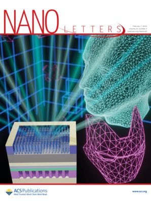
Now, recent work in Nano Letters reports on the development of a sleek 3D surface imaging system with simplified and flatter optics compared to some predecessors, enabling more advanced and efficient facial recognition capabilities.1 This novel system works by employing photonic crystal surface-emitting lasers (PCSELs) and a metasurface hologram to generate structured light—an innovation that builds upon previous work by the team.2,3
Read the Full Article
Metasurface- and PCSEL-Based Structured Light for Monocular Depth Perception and Facial Recognition
Wen-Cheng Hsu, Chia-Hsun Chang, Yu-Heng Hong*, Hao-Chung Kuo*, and Yao-Wei Huang*
DOI: 10.1021/acs.nanolett.3c05002
DOI: 10.1021/acs.nanolett.3c05002
Unlike conventional dot projectors, which rely on diffractive optical elements and collimators, this new system projects around 45,700 infrared dots from a compact 297-μm-dimention metasurface. In practice, this means 1.43 times more spots in a device 233 times smaller than the dot projector in an iPhone. Additionally, it requires up to 10 times less power. In proof-of-concept demonstrations, the new system recognized the face of Michelangelo’s David just as well as an existing smartphone system. This new device and its remarkable advantages in size and power efficiency opens the door to compact integration into wearable devices, with potential for widespread adoption.
Taking a Closer Look at Metasurfaces
Unsurprisingly, these kinds of optical metasurfaces are gaining a lot of attention. But what are metasurfaces? In brief, they are 2D elements or sheets of metamaterials, which are described in this Chemical Reviews Editorial as "artificially designed structures with subwavelength, atomic- or molecular-level constituents that exhibit exotic properties not occurring in nature."4 The resulting metasurfaces can be used to control light by bending or focusing it to generate complex holograms and wavefronts, or to control polarization with high spatial resolution.
A 2024 Roadmap published in ACS Photonics charts the rise of metasurfaces and describes the unique functionalities offered for a variety of uses including imaging, beam forming, holography, and polarimetry, with the potential for significant scientific and industrial impact.5 The first theoretical discussions around these materials date back to the 1940s, but practical development is much more recent, and driven primarily by advances in nanotechnology and semiconductors.

Read the Full Article
Roadmap for Optical Metasurfaces
Arseniy I. Kuznetsov*, Mark L. Brongersma*, Jin Yao, Mu Ku Chen, Uriel Levy, Din Ping Tsai, Nikolay I. Zheludev, Andrei Faraon, Amir Arbabi, Nanfang Yu, Debashis Chanda, Kenneth B. Crozier, Alexander V. Kildishev, Hao Wang, Joel K. W. Yang, Jason G. Valentine, Patrice Genevet, Jonathan A. Fan, Owen D. Miller, Arka Majumdar, Johannes E. Fröch, David Brady, Felix Heide, Ashok Veeraraghavan, Nader Engheta, Andrea Alù, Albert Polman, Harry A. Atwater, Prachi Thureja, Ramon Paniagua-Dominguez, Son Tung Ha, Angela I. Barreda, Jon A. Schuller, Isabelle Staude, Gustavo Grinblat, Yuri Kivshar, Samuel Peana, Susanne F. Yelin, Alexander Senichev, Vladimir M. Shalaev, Soham Saha, Alexandra Boltasseva, Junsuk Rho, Dong Kyo Oh, Joohoon Kim, Junghyun Park, Robert Devlin, and Ragip A. Pala
DOI: 10.1021/acsphotonics.3c00457
DOI: 10.1021/acsphotonics.3c00457
On a slightly larger scale than unlocking your smartphone, metasurfaces are also being investigated in metalenses that could provide a new way to explore the cosmos.6 Incredibly, researchers have created a metalens just 10 cm across—but containing 18.7 billion nanostructures—which is capable of imaging celestial objects in the visible wavelength range. This work overcomes previous exposure area constraints of lithography tools and demonstrates that large metasurfaces are commercially feasible. As new research sheds light on the potential capabilities of metasurfaces and unveils opportunities for improvement in everyday applications, the future of optical technology seems brighter and more accessible than ever.
References
- Hsu, W.-C. et al. Metasurface- and PCSEL-Based Structured Light for Monocular Depth Perception and Facial Recognition. Nano Lett. 2024, 24, 5, 1808–1815.
- Chen, L.-R. et al. Static Beam Steering by Applying Metasurfaces on Photonic-Crystal Surface-Emitting Lasers. J. Light. Technol. 2022, 40 (21), 7136–7141.
- Hsu, W.-C. et al. Compact Structured Light Generation Based on Meta-Hologram PCSEL Integration. Discovery Nano 2023, 18 (1), 87.
- Qiu, C.-W. and Odom, T. W. Introduction: Chemistry of Metamaterials. Chem. Rev. 2022, 122, 19, 14987–14989.
- Kuznetsov, AI, et al. Roadmap for Optical Metasurfaces. ACS Photonics 2024, 11, 3, 816–865.
- Park, J.-S. et al. All-Glass 100 mm Diameter Visible Metalens for Imaging the Cosmos. ACS Nano 2024, 18, 4, 3187–3198.
